
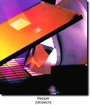
 This image shows a photolithographic stepper, which is used to put patterns on semiconductor wafers using a photographic process. The wafers are coated with a light-sensitive resist, and the patterns that define a chip are developed into the resist by shining light through a pattern mask, as shown.
Once the resist patterns are developed, the exposed patterns on the wafer can be etched, doped, or otherwise chemically modified to create thousands of transistors.
This image shows a photolithographic stepper, which is used to put patterns on semiconductor wafers using a photographic process. The wafers are coated with a light-sensitive resist, and the patterns that define a chip are developed into the resist by shining light through a pattern mask, as shown.
Once the resist patterns are developed, the exposed patterns on the wafer can be etched, doped, or otherwise chemically modified to create thousands of transistors.
A chip manufacturer would use a stepper, like the one shown here, to step many hundreds of wafers per hour through this process using the same mask.
Photograph courtesy of the The Fullman Company