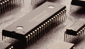

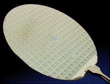
 On the right is a very thin (several hundred microns) slice of crystalline silicon. The pattern on it is a collection of chips which are produced by a photographic process. Each small square in the pattern is a complete chip containing thousands of transistors. These will be broken apart (called cleaving), and each one will be put into a plastic package with metal leads (shown below). These packages can then be used to incorporate the tiny chips into larger circuit boards.
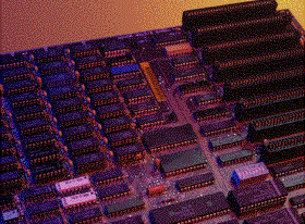
A chip may be a CPU, or Memory, or some other subcomponent of a computer.