Lab #10 (04/11/02)
Adding memory to the 6800 Kit.
© D. Thiébaut
![]() CSC270
Lab #10
CSC270
Lab #10
Experiment #1: Adding a 2114 RAM chip to the Kit.
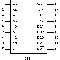
The 2114 is a 1Kx4 RAM circuit. It contains 1024 nybbles. Its pin-out is shown in Figure 1 below.
Your goal is to attach one such circuit to the 6800 processor.
We will use just one, although two are required to implement a memory of bytes. But the wiring of the second RAM chip is identical to the wiring of the first one, except that it connects to four different bits of the data bus. You will simply have to be careful which bits of the data bus you connect to, so that you will know which nybble (high or low) the processor accesses.
Block Diagram
Figure 3 shows the block diagram that you have to complete before you can wire up the kit. Although not much is required to connect the 6800 to the 2114, this can be tricky, and we will take each step one at a time.
Decoding
The CS' signal (also called CE') controls access to the RAM chip (Chip Select), and it must be activated only when the processor is outputting an address corresponding to that circuit. You need to figure out how to select appropriate bits of the address bus to enable this RAM, knowing that the 64K address range of the HeathKit is divided into several fields corresponding to different devices, as shown below.
| Address (Binary) | Address (Hex) | Device |
|---|---|---|
|
1111 1111 1111 1111 1111 1100 0000 0000 |
FFFF FC00 |
ROM |
|
1111 1011 1111 1111 1100 0010 0000 0000 |
FBFF C200 |
Available |
|
1100 0001 1111 1111 1100 0001 0111 0000 |
C1FF C170 |
Not usable |
|
1100 0001 0110 1111 1100 0001 0001 0000 |
C16F C110 |
Display |
|
1100 0001 0000 1111 1100 0000 0000 1111 |
C10F C00F |
Not usable |
|
1100 0000 0000 1110 1100 0000 0000 0011 |
C00E C003 |
Keyboard |
|
1100 0000 0000 0010 1100 0000 0000 0000 |
C002 C000 |
Not usable |
|
1011 1111 1111 1111 0000 0010 0000 0000 |
BFFF 0200 |
Available |
|
0000 0001 1111 1111
0000 0000 0000 0000 |
01FF 0000 |
RAM |
A 3-to-8 decoder is available to decode blocks of addresses: the 7442. Its diagram is shown below:
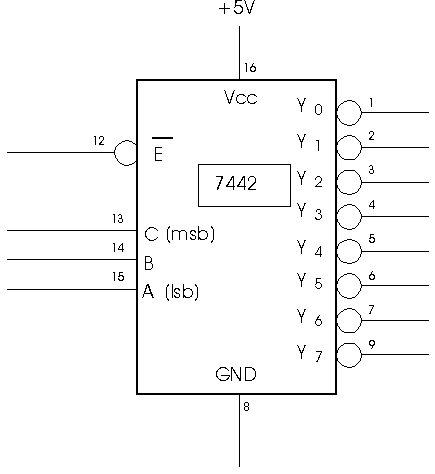
Add the decoder to Figure 3. Figure out what address bits to connect to the three inputs of the decoder, and select an output that is energized by an address that does not map to anything already associated with memory or I/O devices (RAM, ROM, Keyboard, Display, Unavailable), and connect it to the Chip-Select signal (CS') of your RAM circuit.
Find out what signals should be used to energize the (active-low) enable input of the decoder. Wire up the enable input.
Since the 2114 contains 1024 different memory words, you have to make sure that the enable signal you selected can be energized by 1024 different addresses. Furthermore, these 1024 addresses should not overlap with anything already in use (RAM, ROM, I/O).
Verify that this is the case, and indicate why in your report.
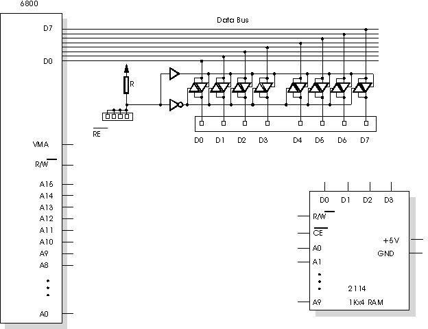
You have to add the decoder and the hardware controlling the tri-state buffers.
Data Bus Connection
Connecting to the data bus must be done via the tri-state buffers. Although the RAM has tri-state buffers internally, and we could have connected its data Input/Output pins directly to the data bus, the kit is designed in such a way that the blocks marked D0, D1, D2, ..., D7 into which you connect wires are connected to additional tri-state drivers and not to the Data Bus. The main reason for this is security. If your design is flawed, all you will destroy is the tri-state drivers, but not the processor!
Connect the DQ signals of the 2114 to the tri-state drivers in Figure 3.
R/W' signal
The R/W' input signal of the 2114 just happens to be of the same polarity as the R/W' signal of the processor. A 1 indicate a processor read operation, a 0 a processor write. Connect the two together on Figure 3.
Address lines
The 2114 contains 1024 words of memory, hence its 10 address input lines. Which address bits from the processor should you connect to the address inputs of the 2114? Why? With your connection established in Figure 3, what is the address of the first word of the RAM? What is the address of the last word of the RAM?
Energizing the R/E' signal
The signal RE' controls the tri-state drivers. Energizing it is the trickiest and most crucial element of the design. If it is not implemented correctly, RE' will activate the tri-state drivers at the wrong time and will force them to output information on the data bus at the same time the processor uses the bus for some other purpose. This conflict will make the processor read erroneous information, and the computer will very likely crash!
Moreover, a few seconds of this bad treatment would be long enough to make some circuits die. (Note: Out of curiosity, at least 2 years ago, the price of 6800 processors was checked. They are hard to find, but a great bargain, at year 2000's price of $2.50 a piece! A significant difference with two year ago's price of $800.00 for a 700-MHz pentiums. Today we can purchase a 1GHz Pentium III chip for $135. )
To find the exact formula for activating RE', use the information in Table 2 to complete Table 3.
| R/E' | Action |
|---|---|
| 0 | Lets information on Data Bus Block flow through tri-state drivers onto Data Bus, so that 6800 can read information into accumulator. |
| 1 | Lets information on data bus go through tri-state drivers to Data Bus Block (where you can connect wires) Table 1. |
| Enable' from decoder (to RAM) |
R/W' from processor |
Behavior of 2114 | R/E' |
|---|---|---|---|
| 0 | 0 | ||
| 0 | 1 | ||
| 1 | 0 | ||
| 1 | 1 |
Once you have found the truth table for RE', generate its boolean equation in terms of the enable' signal from the decoder (going to the RAM), and R/W'. Add the circuit to Figure 3.
Before wiring the circuit, check it with me first!
Wire-up the whole circuit.
Testing
How can you test that your memory is working properly? Run a test to show that you can actually store information in the RAM and retrieve it.