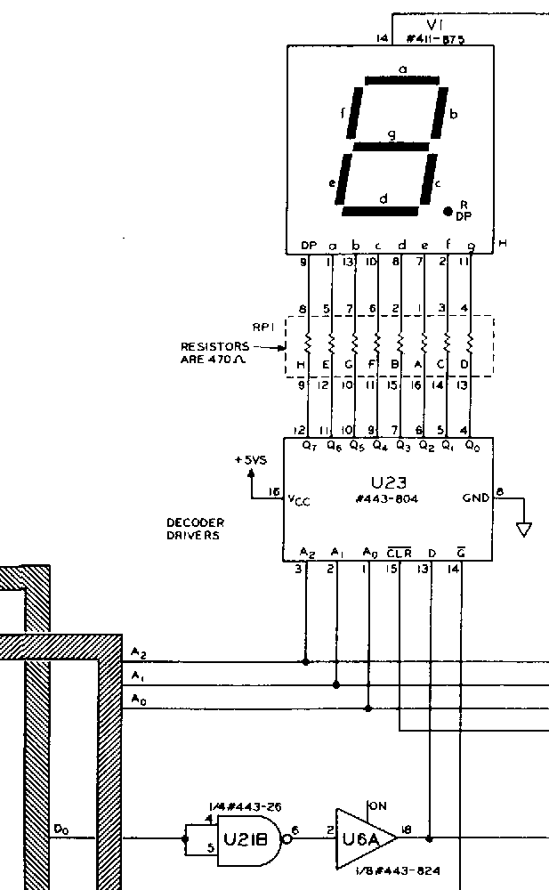
           Leftmost display digit:  0C16Fh
                    second digit:   0C15Fh
                    third digit:    0C14Fh
                    fourth digit:   0C13Fh
                    fifth digit:    0C12Fh
           rightmost display digit: 0C11Fh
Note that we do not know for sure which LED these addresses correspond
to, yet...
Checking the segments
As we saw in class, there should be a jumper, or two posts on the
mother board of the kit allowing us to clear the flipflops
all at once. This will/should turn all the LEDs ON at once.
Look for two posts labeled ST1
and ST2 on the board, and connect
them temporarily with a wire. Do you observe all the segments turning
on?
First programming task: Blinking LED
Your next task is to write a small program that will turn one of the LED
segments of the first LED block ON and OFF. We will start with
Address 0C16Fh.
The idea is to store a 1 (01h) at that address, wait about 1/10th of a second,
then store 0 (00h), wait 1/10th of a second and repeat. The result is an LED
blinking at a rate of 1/0.1s = 10 Hz.
Which LED responds to Address 0C16Fh? _______________
Modify your program and use Address 0C16Eh instead of 0C16Fh. Do not
modify anything else. What LED does the program activate now?
Continue on decrementing the addresses and figure out the
assignment of addresses to LEDs:
            Address of LED a:  ___________
            Address of LED b:  ___________
            Address of LED c:  ___________
            Address of LED d:  ___________
            Address of LED e:  ___________
            Address of LED f:  ___________
            Address of LED g:  ___________
            Address of LED DP: ___________
Next programming task: Displaying 3 on the leftmost digit
Your next task is to write a program that starts with an 8-bit
binary pattern in Acca representing the display of the decimal 3
on the leftmost 7-segment display. The program then stores this
pattern, one bit at a time, on all 8 segments (Hints: look up
the rotate and shift instructions).
Be efficient and use the Index register to hold the address of the LEDs!
Also, use a procedure to display the contents of Acca on a 7-segment
digit. Here is the skeleton and specification of such procedure:
            ;------------------------------------------
            ;OUTPUT: takes the pattern stored in Acca
            ;        and stores in on the 7 segment
            ;        display whose address is passed in
            ;        the X register.
            ;------------------------------------------
            Output:   ...
                      ...
                      ...
                      RTS
With this procedure, displaying a character should be a fairly
simple task. Look at the following example (which might or might
not work with your procedure, depending on how you coded it):
                      LDAA     # 5Bh       ;pattern for digit '5'
                      LDX      # 0C158h    ;address of second digit
                      JSR      Output      ;output pattern on digit
Name that task: Displaying your name on the digits
Now that you have your output procedure working, write a program
that uses it to output your name on the display. You may
shorten your name if you wish!
Experiment #2: A 2-bit output port
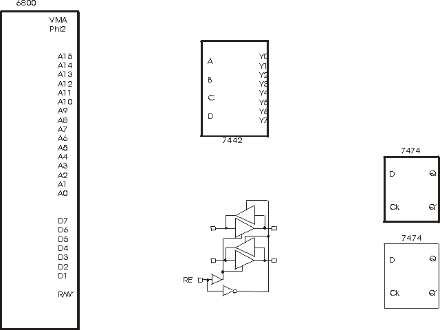
Figure 1: The main players.
Figure 1 shows the main components of the two-bit output port setup.
The 6800, a decoder, two bidirectional buffers controlled by RE-bar,
and two D-flipflops (the sn54/74LS74),
the outputs of which are connected to two LEDs.
Your job is to figure out how to wire them up so that the processor
can store two bits in the port, and activate the LEDs according to the
values of the bits.
As with the RAM lab, you have to make two types of connections: static and
dynamic. The static connections correspond to the data path: How do you
get the bits from the processor to the flipflop?
The dynamic connections correspond to timing-specific issues: How
can you be sure that the data comming from the processor will be
latched in the flipflop at the right time, and only when the processor is
outputing these two bits, and not at other times?
Let's start with the static connections first:
Static connections: Data Path
Static connections: Address Selection
The next action item is to figure out an address (or several) that is
not assigned to any of the other devices on the kit, and to reserve
it for your 2-bit port.
The table below shows the assignment of
addresses used by the Kit. The only addresses that are available
to you are the
ones marked as Available.
| Address (Binary) |
Address (Hex) |
Device |
1111 1111 1111 1111
1111 1100 0000 0000 |
FFFF
FC00 |
ROM |
|---|
1111 1011 1111 1111
1100 0010 0000 0000 |
FBFF
C200 |
Available |
|---|
1100 0001 1111 1111
1100 0001 0111 0000 |
C1FF
C170 |
Not usable |
|---|
1100 0001 0110 1111
1100 0001 0001 0000 |
C16F
C110 |
Display |
|---|
1100 0001 0000 1111
1100 0000 0000 1111 |
C10F
C00F |
Not usable |
|---|
1100 0000 0000 1110
1100 0000 0000 0011 |
C00E
C003 |
Keyboard |
|---|
1100 0000 0000 0010
1100 0000 0000 0000 |
C002
C000 |
Not usable |
|---|
1011 1111 1111 1111
0000 0010 0000 0000 |
BFFF
0200 |
Available |
|---|
0000 0001 1111 1111
0000 0000 0000 0000 |
01FF
0000 |
RAM |
|---|
Table 1: Memory map of 6800 Kit.
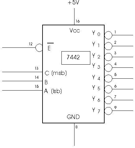 Figure 2: The 7442 used as a 3-to-8 decoder.
You will use the 7442 as a 3-to-8 decoder to help you select a free address
range. The 7442 is shown in Figure 2.
Looking at Table 1, select an address that is available,
and wire up the 7442 to activate one of its outputs when the address
is present on the address bus.
Can you use the same address you used for the RAM during last week's
lab? Why?
Dynamic Connection: latching the 2 bits in the flipflops
Complete the timing diagram shown below and show how the different
signals behave during a processor cycle.
Of interest is a cycle when the 6800 outputs
the 2 data bits to the port, and at the same time outputs on the
address bus the address
you selected in the previous section.
Yi represents the output
of the decoder that is energized by the address of the fliplfops. Dm
and Dn are the two data bits from the data bus that are connected
to the flipflops. Clock is the clock signal fed to the two
flipflops. For this signal, indicate when a low-to-high transition would
be appropriate for it to capture the two data bits. In other words,
indicate the range of time during which it would be okay for it to
go from low to hight.
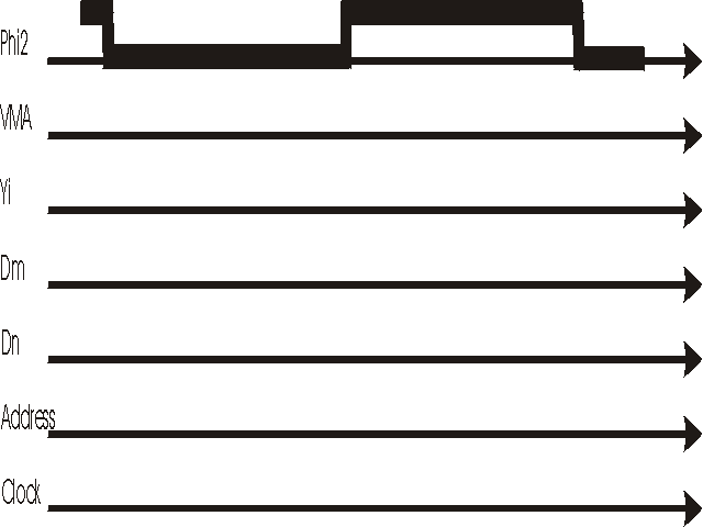 Figure 3: Timing diagram of the main signals
Once the timing diagram is complete, figure out how to generate the
clock signal of the two flipflops.
Testing your circuit
To test your circuit, write a program that shows all combinations of two bits
on the LEDs. Your program should be an endless loop that stores
00, 01, 10, 11,
00 and so on in the flipflops (which now act as a 2-bit I/O
controller, or 2-bit port).
Write your program so that the LED patterns
remain visible for about 2 tenths of a second before a new pattern is
stored in the 2-bit port.